Effect of Substrate Temperature on Structural and Optical Properties of CdO Thin Films
Article Sidebar
Main Article Content
Abstract
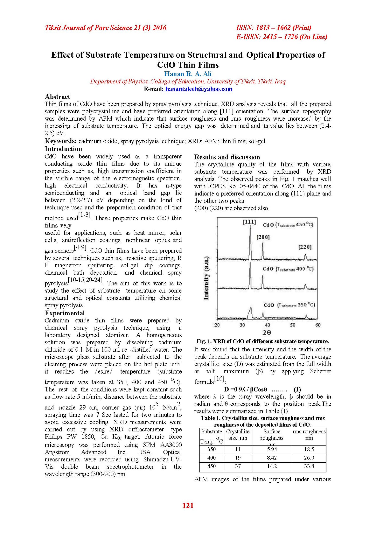
Thin films of CdO have been prepared by spray pyrolysis technique. XRD analysis reveals that all the prepared samples were polycrystalline and have preferred orientation along [111] orientation. The surface topography was determined by AFM which indicate that surface roughness and rms roughness were increased by the increasing of substrate temperature. The optical energy gap was determined and its value lies between (2.4-2.5) eV.
Article Details

This work is licensed under a Creative Commons Attribution 4.0 International License.
Tikrit Journal of Pure Science is licensed under the Creative Commons Attribution 4.0 International License, which allows users to copy, create extracts, abstracts, and new works from the article, alter and revise the article, and make commercial use of the article (including reuse and/or resale of the article by commercial entities), provided the user gives appropriate credit (with a link to the formal publication through the relevant DOI), provides a link to the license, indicates if changes were made, and the licensor is not represented as endorsing the use made of the work. The authors hold the copyright for their published work on the Tikrit J. Pure Sci. website, while Tikrit J. Pure Sci. is responsible for appreciate citation of their work, which is released under CC-BY-4.0, enabling the unrestricted use, distribution, and reproduction of an article in any medium, provided that the original work is properly cited.
References
[1] R. S. Rusu, G. I. Rusu, J. Optoelctronics and Advanced Materials 7 (2005) 1511.
[2] A. A. Dakhel, J. Material Science 46 (2004) 6925.
[3] A. A. Dakhel, A. Y. Ali-Mohamed, J. Sol-Gel Sci. Technol. 44 (2007) 241.
[4] R. Maity, K. K. Chattopadhy, Sol. Energy Mater. Sol. Cells 90 (2006) 597.
[5] B. J. Lokhande, P. S. Patil, M. D. Uplane, Mater. Chem. Phys. 84 (2004) 238.
[6] K. Matsubara, P. Fons, K. Iwata, A. Yamada, K. Sakurai, H. Tampo, S. Niki, Thin Solid Films 341 (2008) 369.
[7] F. Z. Henori, A. A. Dakhel, Laser Phys. 18 (2008) 1557.
[8] R. R Salunkhe, D. S. Dhawala, P. P. Dunai, C. D. Lokhande, Sens. Actuators B 140 (2009) 86.
[9] R. Srinivasaraghavan, R. Chandiramouli, B. G. Teyaprakosh, S. Seshadri, Spectrochimica Acta Part A: Molecular and Bio Molecular Spectroscopy 102 (2013) 242.
[10] N. Ueda, H. Maeda, H. Ozono, H. K. Awazoe, J. Appl. Phys. 84 (1998) 6174.
[11] Wei-Min Cho, Guan-Ru He, Ting-Hong Su, Yow-Jon Jin, Applied Surface Science 258(2012) 4632.
[12] A. A. Ziabari, F. E. Ghodsi, G. Kiriakidis, Surface Coating Technology 213 (2012) 15.
[13] A. S. Kamble, R. C. Pawar, J. Y. Patil, S. S. Suryavanshi, P. S. Patil, J. Alloy Comp.
509 (2011) 1035.
[14] D. lanb, S. J. C. Irvine, J. Cryst. Growth 332 (2011) 17.
[15] V. Biligin, I. A kyuz, S. Kose, F. Atay, Semicond. Sci. Technol. 21 (2006) 579.
[16] E. F. Kaelble, Handbook of X-rays for diffraction,emission, absorption, and
microscopy. McGraw-Hill, New York, (1967) p. 5.
[17] Sudjaatmoko, Wirjoadi, B. Siswanto, Atom Indonesia 35 (2009) 115.
[18] M. R. A. Bhyiyan, M. A. H. Miah, J. Begum, J. Bangladesh Academy of Science
36 (2012) 233.
[19] J. Tauc, Amorphous and Liquid Semiconductors, Plenum Press London, 1974.
[20] Nadir Fadhil Habubi, Sami Salmann Chiad, Saad Farhan Oboudi, Ziad Abdulahad
Toma, International Letters of Chemistry, Physics and Astronomy 4 (2013) 1-8.
[21] Saad F. Oboudi, Nadir F. Habubi, Ghuson H. Mohamed, Sami S. Chiad, International Letters of Chemistry, Physics and Astronomy 8(1) (2013) 78-86.
[22] J. A. Najim, J. M. Rozaiq, International Letters of Chemistry, Physics and Astronomy10(2) (2013) 137-150.
[23] Majid H. Hassouni, Khudheir A. Mishjil, Sami S. Chiad, Nadir F. Habubi, International Letters of Chemistry, Physics and Astronomy 11 (2013) 26-37.
[24] K. K. Patankar, International Letters of Chemistry, Physics and Astronomy 1 (2014) 1-8.