Preparation CdSe thin films by vacuum thermal evaporation and studying the effect of annealing time on structural, electrical and optical properties.
Article Sidebar
Main Article Content
Abstract
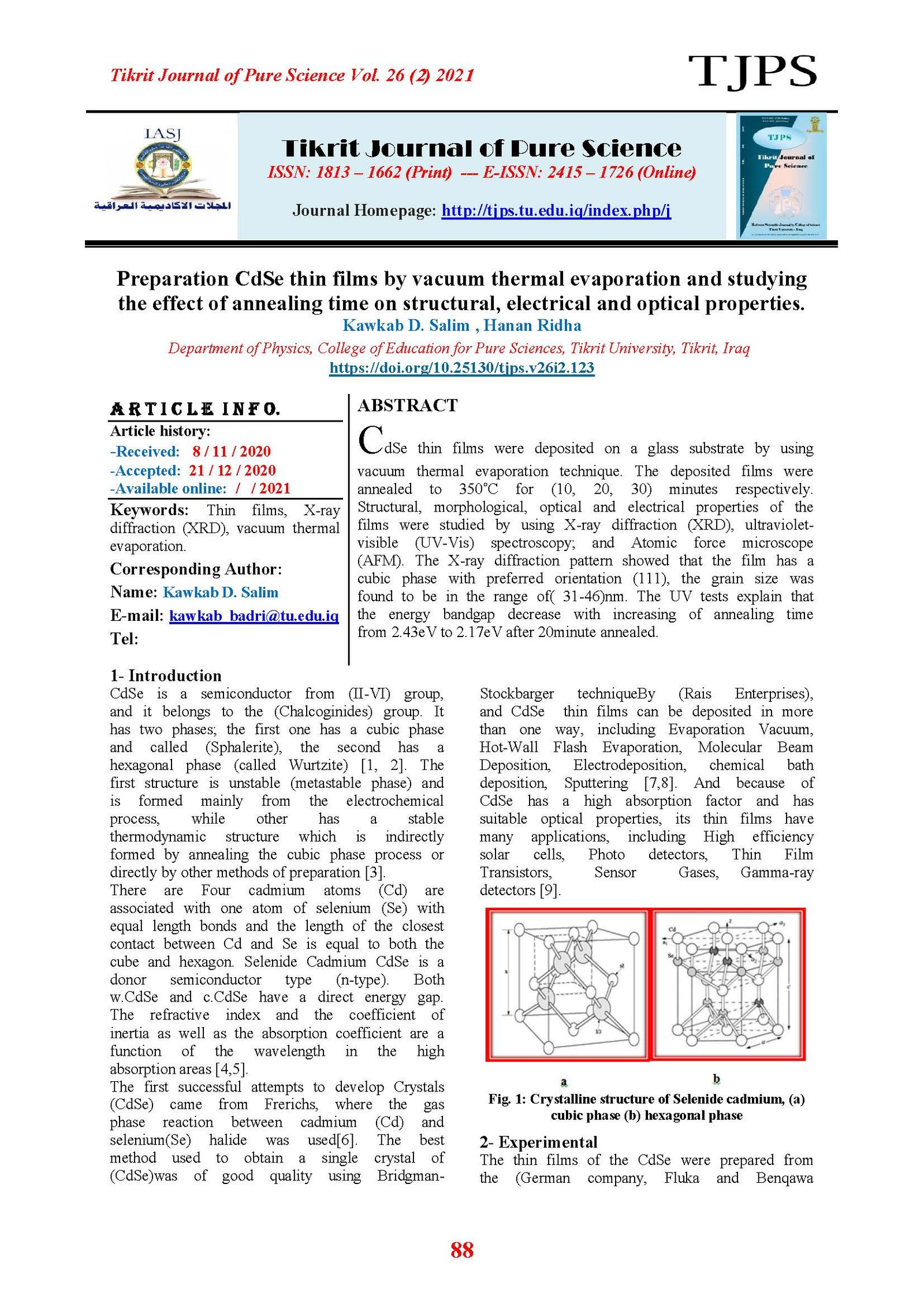
CdSe thin films were deposited on a glass substrate by using vacuum thermal evaporation technique. The deposited films were annealed to 350˚C for (10, 20, 30) minutes respectively. Structural, morphological, optical and electrical properties of the films were studied by using X-ray diffraction (XRD), ultraviolet-visible (UV-Vis) spectroscopy; and Atomic force microscope (AFM). The X-ray diffraction pattern showed that the film has a cubic phase with preferred orientation (111), the grain size was found to be in the range of( 31-46)nm. The UV tests explain that the energy bandgap decrease with increasing of annealing time from 2.43eV to 2.17eV after 20minute annealed.
Article Details

This work is licensed under a Creative Commons Attribution 4.0 International License.
Tikrit Journal of Pure Science is licensed under the Creative Commons Attribution 4.0 International License, which allows users to copy, create extracts, abstracts, and new works from the article, alter and revise the article, and make commercial use of the article (including reuse and/or resale of the article by commercial entities), provided the user gives appropriate credit (with a link to the formal publication through the relevant DOI), provides a link to the license, indicates if changes were made, and the licensor is not represented as endorsing the use made of the work. The authors hold the copyright for their published work on the Tikrit J. Pure Sci. website, while Tikrit J. Pure Sci. is responsible for appreciate citation of their work, which is released under CC-BY-4.0, enabling the unrestricted use, distribution, and reproduction of an article in any medium, provided that the original work is properly cited.
References
[1] Tanaka, K. (1989). Structure Phase Transitions in Chalco genide Glasses. Physical Review B, (39): 1270-1279.
[2] Samy, M.K.; Bahadur, S.A. and Murali, K.R. (2009). Photoconductive Studies on Electron Beam Evaporated CdSe Films. Physics B: condensed matter, 404(16): 2449-2454.
[3]Khalaf, M. Kh.; ALhilliy, B.A.M.; Khudiara, A. I.; Abd Alzahra, A. (2016) Influence of nanocrystalline size on optical band gap in CdSe thinfilms prepared by DC sputtering. Photonics and Nanostructures – Fundamentals and Applications, 18: 59–66.
[4] Ismail, R. A.; Habubi, N. F. and Abd, A. N.(2015) Effect of Laser Fluence on the Characteristics of CdSe Nanoparticles Prepared by Laser Ablation in Methanol. High Energy Chemistry, 49(6): 438–448.
[5] Rosmani, C. H.; Zainurul, A. Z.; Rusop, M. and Abdullah, S. (2014) The Optical and Electrical Properties of CdSe Nanoparticles. Advanced Materials Research 832: 557-561.
[6] Thirumavalavan, S.; Mani, K. and Suresh S. (2015) Structural, Surface Morphology, Optical and elictrical investigation of CdSe Thin films. Materials Research, 12( 5): 237 – 246.
[7] Dler, J. (2015). Thin Film Deposition Processes. International Journal of Modern Physics and Applications, 1(4):193-199.
[8] Lofgran, S.C. (2013). Thin film Deposition and vacuum technology, Master thesis, Brighan yong University, Idaho, USA: 3pp.
[9] Surana, K.; Singh, P. K.; Rhee, Hee-Wand Bhattacharya, B. (2016) Synthesis,
characterization and application of CdSe quantum dots. Material Sci Eng, 5(6): 4188-4193.
[10] Yu, D. et.al. (2006). Electronic transport of n-type CdSe quantum dot films: Effect of film treatment. Journal of applied physics, 99(104315):1-7
[11] Bathusha, S. et.al (2016). Effect of Temperature of Electron Beam Evaporated CdSe Thin Films. Material Sci Eng 2016, 5(6):1-5.