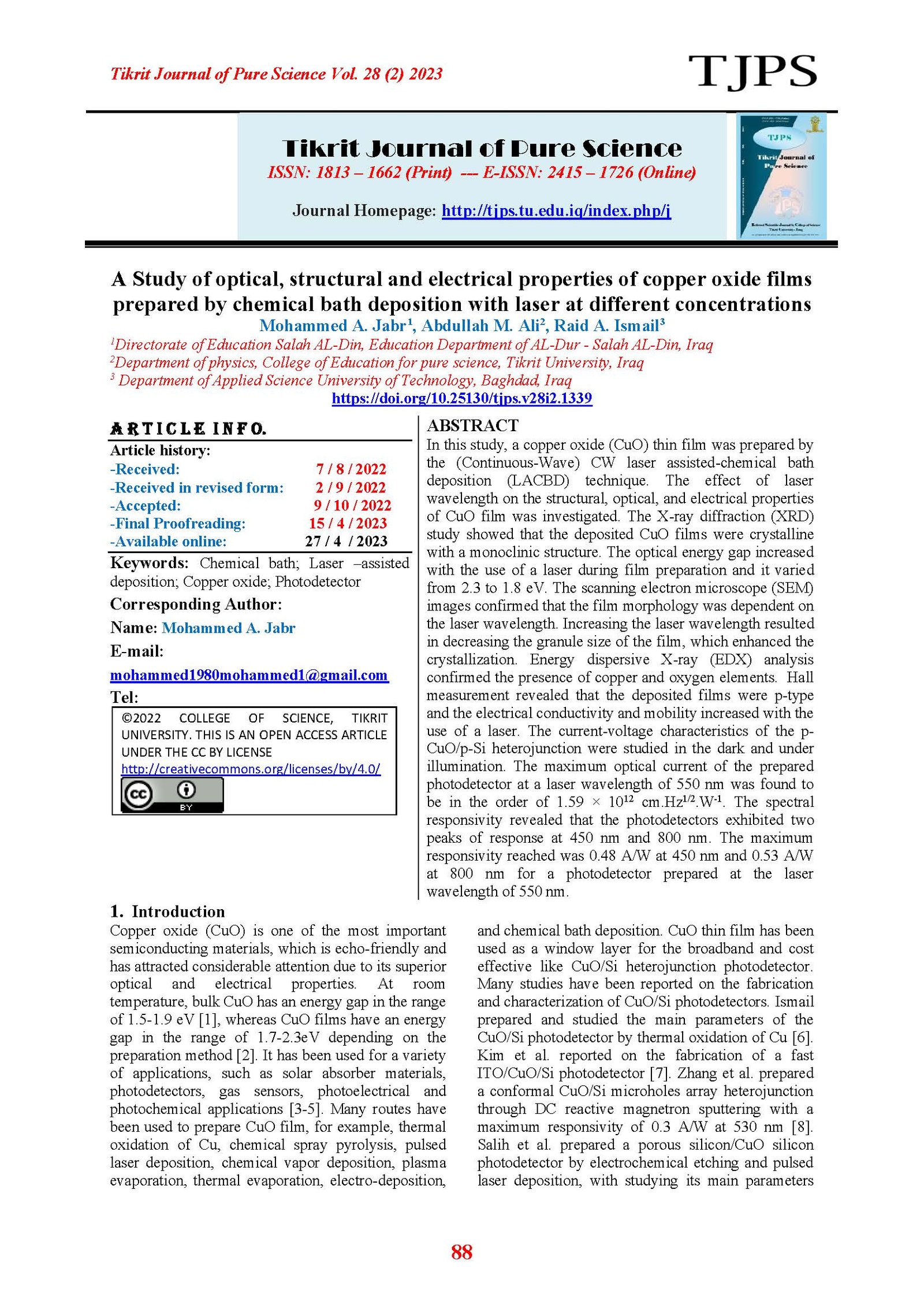
A Study of optical, structural and electrical properties of copper oxide films prepared by chemical bath deposition with laser at different concentrations
Main Article Content
Abstract
In this study, a copper oxide (CuO) thin film was prepared by the (Continuous-Wave) CW laser assisted-chemical bath deposition (LACBD) technique. The effect of laser wavelength on the structural, optical, and electrical properties of CuO film was investigated. The X-ray diffraction (XRD) study showed that the deposited CuO films were crystalline with a monoclinic structure. The optical energy gap increased with the use of a laser during film preparation and it varied from 2.3 to 1.8 eV. The scanning electron microscope (SEM) images confirmed that the film morphology was dependent on the laser wavelength. Increasing the laser wavelength resulted in decreasing the granule size of the film, which enhanced the crystallization. Energy dispersive X-ray (EDX) analysis confirmed the presence of copper and oxygen elements. Hall measurement revealed that the deposited films were p-type and the electrical conductivity and mobility increased with the use of a laser. The current-voltage characteristics of the p-CuO/p-Si heterojunction were studied in the dark and under illumination. The maximum optical current of the prepared photodetector at a laser wavelength of 550 nm was found to be in the order of 1.59 × 1012 cm.Hz1/2.W-1. The spectral responsivity revealed that the photodetectors exhibited two peaks of response at 450 nm and 800 nm. The maximum responsivity reached was 0.48 A/W at 450 nm and 0.53 A/W at 800 nm for a photodetector prepared at the laser wavelength of 550 nm.
Article Details

This work is licensed under a Creative Commons Attribution 4.0 International License.
Tikrit Journal of Pure Science is licensed under the Creative Commons Attribution 4.0 International License, which allows users to copy, create extracts, abstracts, and new works from the article, alter and revise the article, and make commercial use of the article (including reuse and/or resale of the article by commercial entities), provided the user gives appropriate credit (with a link to the formal publication through the relevant DOI), provides a link to the license, indicates if changes were made, and the licensor is not represented as endorsing the use made of the work. The authors hold the copyright for their published work on the Tikrit J. Pure Sci. website, while Tikrit J. Pure Sci. is responsible for appreciate citation of their work, which is released under CC-BY-4.0, enabling the unrestricted use, distribution, and reproduction of an article in any medium, provided that the original work is properly cited.
References
[1] Morigaki, K. (1999). Physics of amorphous semiconductors. Singapore, World Scientific: 432 pp.
[2] Ogwu, A.A.; Darma, T.H. and Bouquerel, E. (2007). Electrical resistivity of copper oxide thin films prepared by reactive magnetron sputtering. Journal of achievements in materials and manufacturing engineering, 24(1):172–177.
[3] Bakanski, M. and Wallis, R.F. (2000). Semiconductor physics and application: Series on Semiconductor Science and Technology. United States, Oxford University Press, New York.
[4] Balamurugan, B. and Mehta, B.R. (2001). Optical and structural properties of nanocrystalline copper oxide thin films prepared by activated reactive evaporation. Journal of Thin Solid Films, 396(1-2):90–96.
[5] Aiping, C. et al. (2009). Nonlinear optical properties of laser deposited CuO thin films. Journal of Thin Solid Films, 517(15):4277–4280.
[6] Raed, A.I. (2009). Characteristics of p-Cu₂O/n-Si Heterojunction Photodiode made by Rapid Thermal Oxidation. Journal of Semiconductor Technology and Science, 9(1),51–54.
[7] Kim, S.H.; Kumar, M.D.; Patel, M. and Kim, J. (2016). High-performing ITO/CuO/n-Si photodetector with ultrafast photoresponse, Sensors and Actuators A: Physical, 252(1), 35–41.
[8] Zhang, C. et al. (2021). Enhanced Light Trapping in Conformal CuO/Si Microholes Array Heterojunction for Self-Powered Broadband Photodetection. IEEE Electron Device Letters, 42(6):883–886.
[9] Salih, E.Y.; Mohamed, B.A.; Altaf, H.R. and Irfan, A.B. (2022). Fabrication and characterization of porous Si/CuO film for visible light MSM photodetector: The effect of post-processing temperature. Ceramics International, 48(7):9965–9972.
[10] Garcia, L.V. et al. (2016). Structure and properties of CdS thin films prepared by pulsed laser assisted chemical bath deposition. Materials Research Bulletin, 83:459–467
[11Palema, N. (2016). Growth mechanisms and their effects on the opto-electrical properties of CdS thin films prepared by chemical bath deposition. Materials Science in Semiconductor Processing , 52:24–31.
