Preparation of porous silicon Wafers using sun light photo chemical etching (SLPCE)
Article Sidebar
Main Article Content
Abstract
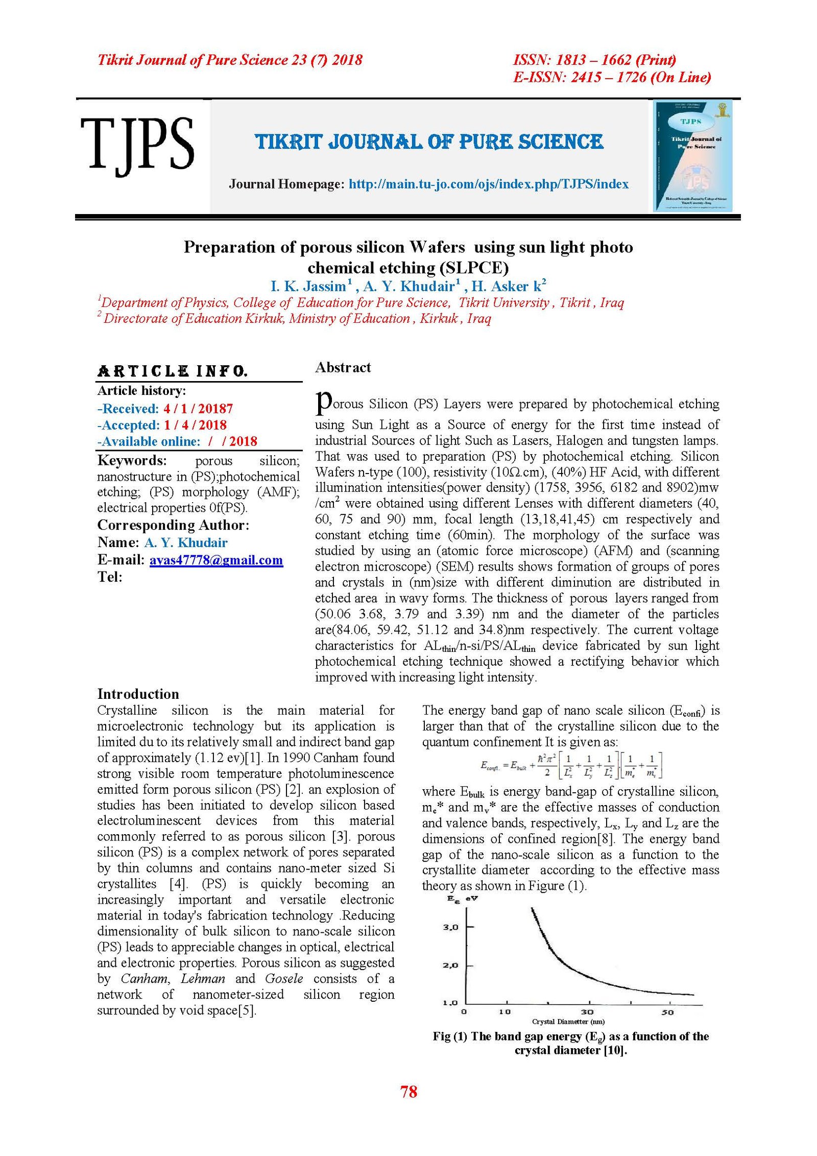
porous Silicon (PS) Layers were prepared by photochemical etching using Sun Light as a Source of energy for the first time instead of industrial Sources of light Such as Lasers, Halogen and tungsten lamps. That was used to preparation (PS) by photochemical etching. Silicon Wafers n-type (100), resistivity (10Ω.cm), (40%) HF Acid, with different illumination intensities(power density) (1758, 3956, 6182 and 8902)mw /cm2 were obtained using different Lenses with different diameters (40, 60, 75 and 90) mm, focal length (13,18,41,45) cm respectively and constant etching time (60min). The morphology of the surface was studied by using an (atomic force microscope) (AFM) and (scanning electron microscope) (SEM) results shows formation of groups of pores and crystals in (nm)size with different diminution are distributed in etched area in wavy forms. The thickness of porous layers ranged from (50.06 3.68, 3.79 and 3.39) nm and the diameter of the particles are(84.06, 59.42, 51.12 and 34.8)nm respectively. The current voltage characteristics for ALthin/n-si/PS/ALthin device fabricated by sun light photochemical etching technique showed a rectifying behavior which improved with increasing light intensity.
Article Details

This work is licensed under a Creative Commons Attribution 4.0 International License.
Tikrit Journal of Pure Science is licensed under the Creative Commons Attribution 4.0 International License, which allows users to copy, create extracts, abstracts, and new works from the article, alter and revise the article, and make commercial use of the article (including reuse and/or resale of the article by commercial entities), provided the user gives appropriate credit (with a link to the formal publication through the relevant DOI), provides a link to the license, indicates if changes were made, and the licensor is not represented as endorsing the use made of the work. The authors hold the copyright for their published work on the Tikrit J. Pure Sci. website, while Tikrit J. Pure Sci. is responsible for appreciate citation of their work, which is released under CC-BY-4.0, enabling the unrestricted use, distribution, and reproduction of an article in any medium, provided that the original work is properly cited.
References
]1[ A .f. Mohammad," study of laser Effects on porous silicon properties " Master Thesis/ department of Applied sciences/ University of Technology(2006).
]2[ S. Jan. S '' production of porous silicon by laser – Induced Etching ''Master Thesis/ department of Applied sciences / University of Technology(2006).
]3[ Mukarram Abdul- mutalib Al-gaafar, "production of porous silicon studying Its Electrical properties". Master thesis /Department of laser and optoelectronic Engineering , University of Technology (2007).
]4[ V. Lehmann, and U. Gosele"porous silicon formation a quantum wire" Appl. Phys. Lett. 58 (1991) 856.
]5[ A.M. Alwan, "Electrical properties of porous silicon prepared By photochemical Etching". XXII Regional conference on solid state science and technology, 18-21, (2005).
]6[ H .Asker .K," preparation and study of porous silicon layers from n-type silicon wafers using different etching techniques "PhD thesis college of science , University of Baghdad(2010).
]7[ Jeyakumaran N, Natarajan B, Ramamurthys. And vasu V, '' structural and optical properties of n-type porous silicon – effect of etching time", I J NN, Vol .3,pp. 1, , 2007
[8] Y.Z. Dawood " preparation of porous silicon and It's Application in solar Cell "Master Thesis
Department of Applied Scinces/ University of Technology (2009).
[9] R.M. Shehab '' preparation and Characterization of Nano Porous silicon for chemical Detection" Master thesis Department of Applied Sciences, University of Technology(2015). ]10[ B.G. Rasheed, "production of poruos silicon by laser - indused etching", India,(2001).